If you are interested in what went into writing this blog post, you can view a replay of the livestream here.
As I’ve been working on the logic design for
moss, I have been regularly investigating
how Vivado
translates the Verilog RTL (Register Transfer Level) source into Basic
Elements of Logic (BELs), a process known as synthesis. BELs represent the
physical components on an FPGA that can be used to implement a design. One of
the larger elements that you will find on most FPGAs is some type of Block RAM
(BRAM). BRAM can be useful when there is a large memory with attributes that
match the physical component, as well as instances where other resources are
being used for implementation of the rest of the design.
I was curious about when Vivado would infer BRAM and when it would not, so I put together a minimal design meant to exercise the synthesis process. The design consists of three modules.
top is the “top” module, which serves to take inputs on package pins for the
FPGA and connect them to child modules. Every design has a top module that
represents its entrypoint.
top.v
module top(
    input clk,
    input [1:0] sw,
    output [1:0] led
    );

    wire [7:0] w_data;
    wire [7:0] r_data;
    wire [7:0] w_addr;
    wire [7:0] r_addr;

    counter counter(.clk(clk), .w_data(w_data), .w_addr(w_addr), .r_addr(r_addr));

    maybe_bram maybe_bram(.clk(clk), .i_addr(w_addr), .i_data(w_data), .o_addr(r_addr), .write(sw[0]), .read(sw[1]), .o_read(r_data));

    // Do something with the data read from bram so that it does not get
    // eliminated in synthesis.
    assign led[0] = r_data > 100 ? 1 : 0;
endmodule
The counter module is only serving to manipulate the values of the signals
that we will be using in our RAM module. It increments each of the passed
signals on a positive clock edge (posedge) until they reach 255, at which
point they are reset to 0.
counter.v
module counter(
    input clk,
    output reg [7:0] w_data,
    output reg [7:0] w_addr,
    output reg [7:0] r_addr
    );

    always @(posedge clk) begin
	    w_data <= w_data == 255 ? 0 : w_data + 1;
	    w_addr <= w_addr == 255 ? 0 : w_addr + 1;
	    r_addr <= r_addr == 255 ? 0 : r_addr + 1;
    end
endmodule
Vivado also specifies attributes that can be placed in RTL to indicate that a signal should not be removed during optimization.
DONT_TOUCH,KEEP, andKEEP_HIERARCHYprovide variations of this functionality.
The final module, maybe_bram, consists of a 256-register array with 8-bit
values and can be read from and written to.
maybe_bram.v
module maybe_bram(
    input clk,
    input [7:0] i_addr,
    input [7:0] i_data,
    input [7:0] o_addr,
    input write,
    input read,
    output reg [7:0] o_read
    );

    reg [7:0] ram [255:0];

    always @(posedge clk) begin
       if (write == 1'b1) begin
	      ram[i_addr] <= i_data;
       end
       if (read == 1'b1) begin
          o_read <= ram[o_addr];
       end
    end
endmodule
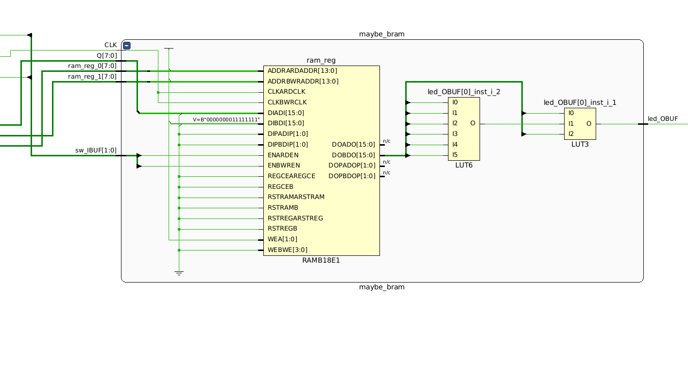
After synthesizing for the Artix
7 FPGA on my
Arty A7 development
board, we can
see that the maybe_bram module consists of a
RAMB18E1
primitive, as well as a
LUT6
and a
LUT3.
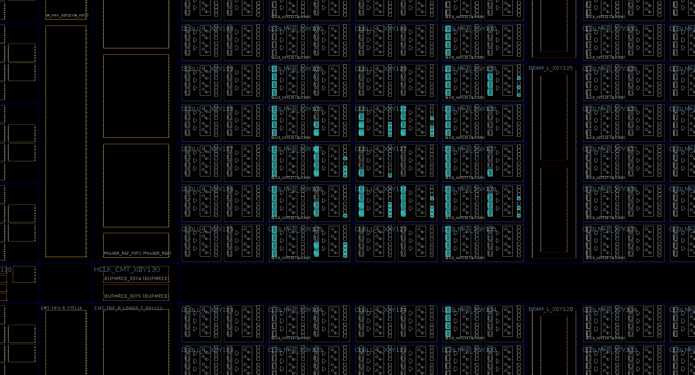
After implementation, which consists of taking the synthesized netlist and mapping the primitives to physical elements on the FPGA, we can see the specific BRAM, LUTs, and other elements used on the device.
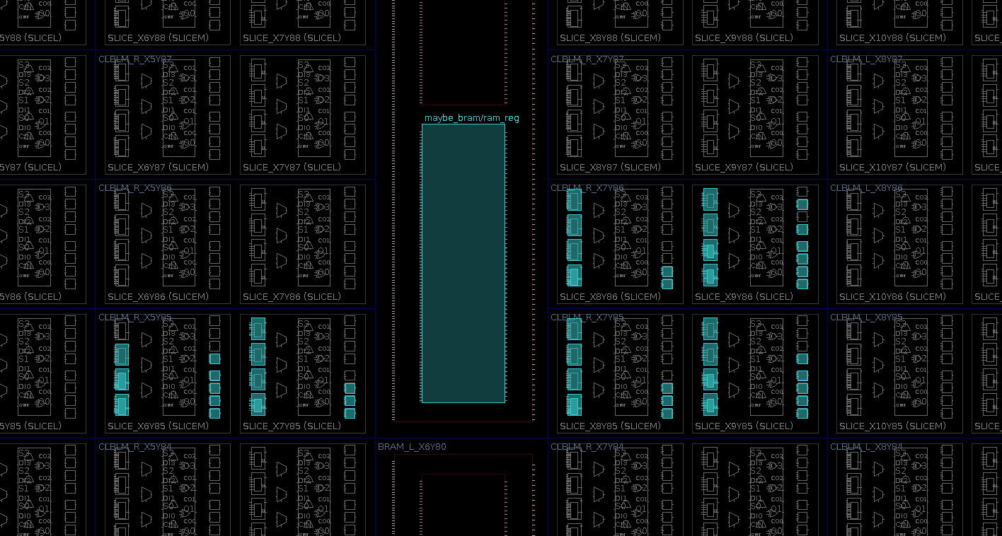
Implementation is commonly referred to as “place and route”.
We are primarily interested in the RAMB18E1 element, which is an 18K-bit
Configurable Synchronous Block RAM. The Xilinx documentation describes this
element as a good choice for FIFO queues, automatic error correction RAM, or
general purpose memory. The B18 refers to the 18K-bit size, while it appears
the E1 suffix refers to the “edition” of the primitive, though I was unable to
confirm that from any official sources.
The
Esuffix is appended to a variety of Xilinx primitives and does not appear to refer directly to any specific functionality. However, newer products seem to have similar primitives with a largerxvalue inEx. For example, the Versal equivalent to theRAMB18E1is theRAMB18E5, which is still 18K-bit, but offers a variety of other features, such as Block RAM Cascading. If you are aware of a more exact definition of theEsuffix feel free to reach out!
Will Green has put together a great guide on FPGA memory types over at Project F if you’re interested in all the variations that different vendors provide. Typically, BRAM and Distributed RAM are compared as options for implementing memories for logic designs on an FPGA.
Distributed RAM makes use of Look-Up Table (LUT) BELs, which are the primary
primitives used to implement custom logic in an FPGA. LUTs typically consist of
static random access memory
(SRAM) and
multiplexers, resulting in an
element that can be configured as any logic function with the specified number
of inputs (e.g. 6 inputs on a LUT6 BEL). BRAM, on the other hand, only acts as
a memory on its own, making it less flexible than LUTs. For this reason,
synthesis tools will frequently opt to use BRAM elements for logic that
implements a memory in order to preserve LUTs for custom logic when possible.
However, there are cases in which the latter is more appropriate than the
former. The Xilinx documentation provides guidance for when to use BRAM or
Distributed
RAM,
which focuses on read and write behavior.
| Action | Distributed RAM | Block RAM |
|---|---|---|
| Write | Synchronous | Synchronous |
| Read | Asynchronous | Synchronous |
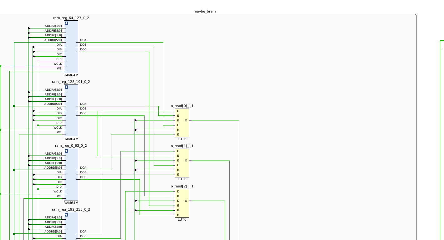
From this information, we can see that there are a number of attributes of our design that would make it a strong candidate to use BRAM.
Reading and writing on the maybe_bram module are clocked.
Link to heading
As shown in the table above, BRAM reads and writes are both synchronous, while
only distributed RAM writes are synchronous. In our maybe_bram module, both
reads and writes occur on the positive edge of the clock (clk), meaning they
are both synchronous. We can test this by converting the read operations to
asynchronous and re-running synthesis and implementation.
maybe_bram.v
module maybe_bram(
    input clk,
    input [7:0] i_addr,
    input [7:0] i_data,
    input [7:0] o_addr,
    input write,
    input read,
    output [7:0] o_read
    );

    reg [7:0] ram [255:0];

    assign o_read = ram[o_addr]; // asynchronous

    always @(posedge clk) begin
       if (write == 1'b1) begin
	      ram[i_addr] <= i_data;
       end
    end
endmodule
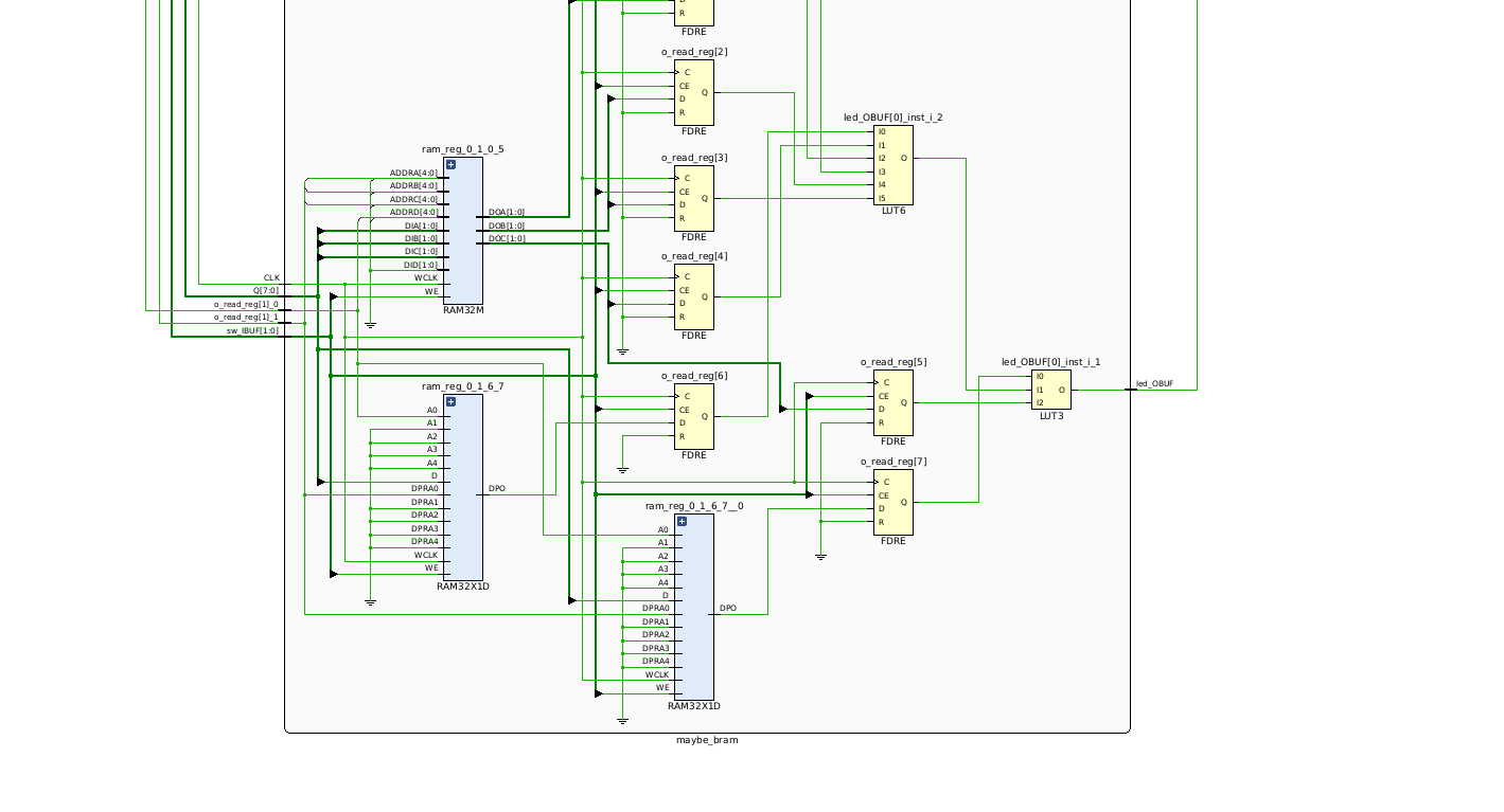
Though only a portion of the schematic is shown in the image below, we can see
that maybe_bram module is now being implemented using multiple RAM64M
elements, which are actually made up of multiple LUT6 BELs.
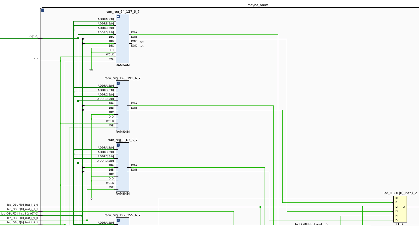
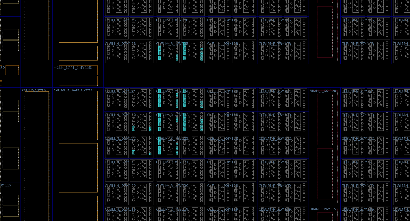
The absence of BRAM usage can also be seen on the device.
Our register array is relatively large. Link to heading
Another reason why BRAM may be selected, or not selected, is due to the size of
the memory. While there are certainly much larger memories that may be
instantiated in a design, ours is at least large enough that it could not be
implemented with a single LUT element. However, if we shrink the size of the
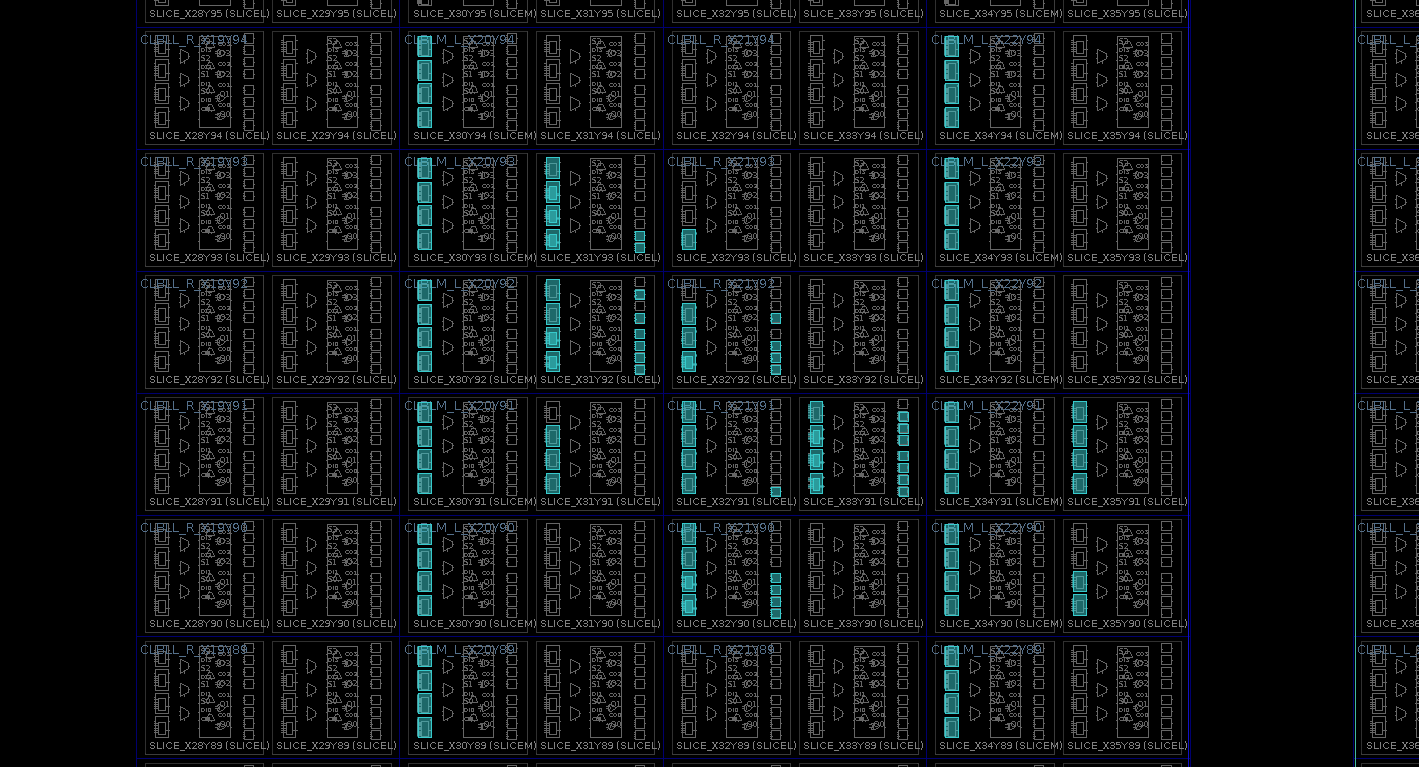
array down to a depth of two (i.e. [1:0]), the initial synchronous read /
synchronous write design will infer distributed RAM using RAM32M and
RAM32X1D elements, which are made up of LUTs.
maybe_bram.v
module maybe_bram(
    input clk,
    input [7:0] i_addr,
    input [7:0] i_data,
    input [7:0] o_addr,
    input write,
    input read,
    output reg [7:0] o_read
    );

    reg [7:0] ram [1:0]; // depth = 2

    always @(posedge clk) begin
       if (write == 1'b1) begin
	      ram[i_addr] <= i_data;
       end
       if (read == 1'b1) begin
          o_read <= ram[o_addr];
       end
    end
endmodule
The implementation is also, expectedly, noticeably smaller than the asynchronous read / synchronous write example.
It is likely that inference behavior could vary based on the usage of elements by other modules in a larger design. Unlike the asynchronous read / synchronous write example, this smaller memory could still be implemented with BRAM. In a future post, I’d like to explore how Vivado responds in more constrained scenarios.
We didn’t explicitly specify a RAM style. Link to heading
We briefly mentioned some of the attributes supported by Vivado earlier, but one
that we didn’t touch on is
RAM_STYLE.
This allows us to guide synthesis in what type of RAM to infer, and if we apply
the distributed value to our synchronous read / synchronous write example, it
will use distributed RAM instead of the BRAM it selected without an attribute.
maybe_bram.v
module maybe_bram(
    input clk,
    input [7:0] i_addr,
    input [7:0] i_data,
    input [7:0] o_addr,
    input write,
    input read,
    output reg [7:0] o_read
    );

    (* ram_style = "distributed" *) reg [7:0] ram [255:0];

    always @(posedge clk) begin
       if (write == 1'b1) begin
	      ram[i_addr] <= i_data;
       end
       if (read == 1'b1) begin
          o_read <= ram[o_addr];
       end
    end
endmodule
The schematic view looks mostly similar to the asynchronous read / synchronous write example.
And the same is true for the device.
Closing Thoughts Link to heading
One of the things I consistently hear from folks working on chip design or FPGAs is to study how the HDL you write is being translated into actual circuits. While I am still in the earlier stages of my journey to develop expertise in chip design, I want to make sure that my learnings (and mistakes) in this area are being captured for others who come after me. If you’re interested in keeping up with this content, subscribe to the RSS feed for this blog, and tune in for my ~weekly livestreams.
As always, if you have feedback, questions, or just want to chat, feel free to
reach out to @hasheddan on any of the platforms listed on the home
page.