If you are interested in what went into writing this blog post, you can view a replay of the livestream here.
In a recent post we explored when Vivado inferred Block RAM (BRAM) for memories in FPGA designs, and when it used distributed RAM instead. While it is somewhat obvious why BRAM can be used for memory in an FPGA (i.e. it is literally a discrete memory element), distributed RAM is a bit more complicated.
Look-Up Tables (LUTs) are a key element of FPGAs that allow it to behave as
“reconfigurable hardware”. Depending on the the size (number of inputs and
outputs) of a LUT, some set of logic functions can be programmed as part of a
design. Understanding how this is possible requires exploring the architecture
of LUT elements. We have been using Xilinx 7 Series
FPGAs while
developing moss, so we’ll focus on them
today. The Xilinx design elements documentation decsribes LUTs as follows.
LUTs are the basic logic building blocks and are used to implement most logic functions of the design.
Xilinx Design Elements Documentation
Internally, LUTs are typically implemented with static random access memory (SRAM) and multiplexers. The SRAM bits are written on FPGA configuration to dictate the outputs when various inputs are supplied. SRAM is the same technology used to implement CPU registers and caches, and is typically faster than dynamic random access memory (DRAM), which has to be periodically refreshed to retain its contents. All About Circuits has a great post on internal architecture of LUTs if you are interested in learning more.
Note: Dynamic Random Access Memory (DRAM) is not to be confused with distributed RAM. The latter is the term used for LUT-based memory in an FPGA, which, somewhat confusingly is being implemented with SRAM. This is why block RAM is sometimes referred to as BRAM, but distributed RAM is not referred to as DRAM.
LUTs can vary in their number of inputs. For example, the diagram below
illustrates a 2-input LUT (LUT2).
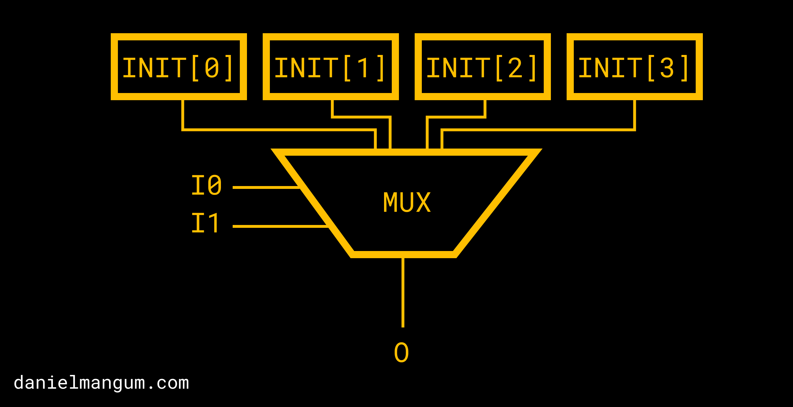
Abstract depiction of a 2-input LUT.
The INIT[X] values refer to those programmed via the FPGA bitstream, while the
I0 and I1 signals represent wires that are dynamically driven high or low.
Those input signals can be thought of as the “selectors” for the multiplexer,
with each permutation selecting a different initial value. Therefore, if we have
4 initial values, we will need 2 input signals to be able to select each of them
(i.e # initial values = 2^(# input signals)).
The ability to set each of the INIT[X] values to 1 or 0 means that we can
implement any truth table. In other
words, we can implement arbitrary logic. The truth table for the LUT2 example
above looks as follows.
| I0 | I1 | O |
|---|---|---|
0 |
0 |
INIT[0] |
0 |
1 |
INIT[1] |
1 |
0 |
INIT[2] |
1 |
1 |
INIT[3] |
Looking back at our example from last post where distributed RAM was used to
implement our design, we can see
RAM32M
and
RAM32X1D
elements.
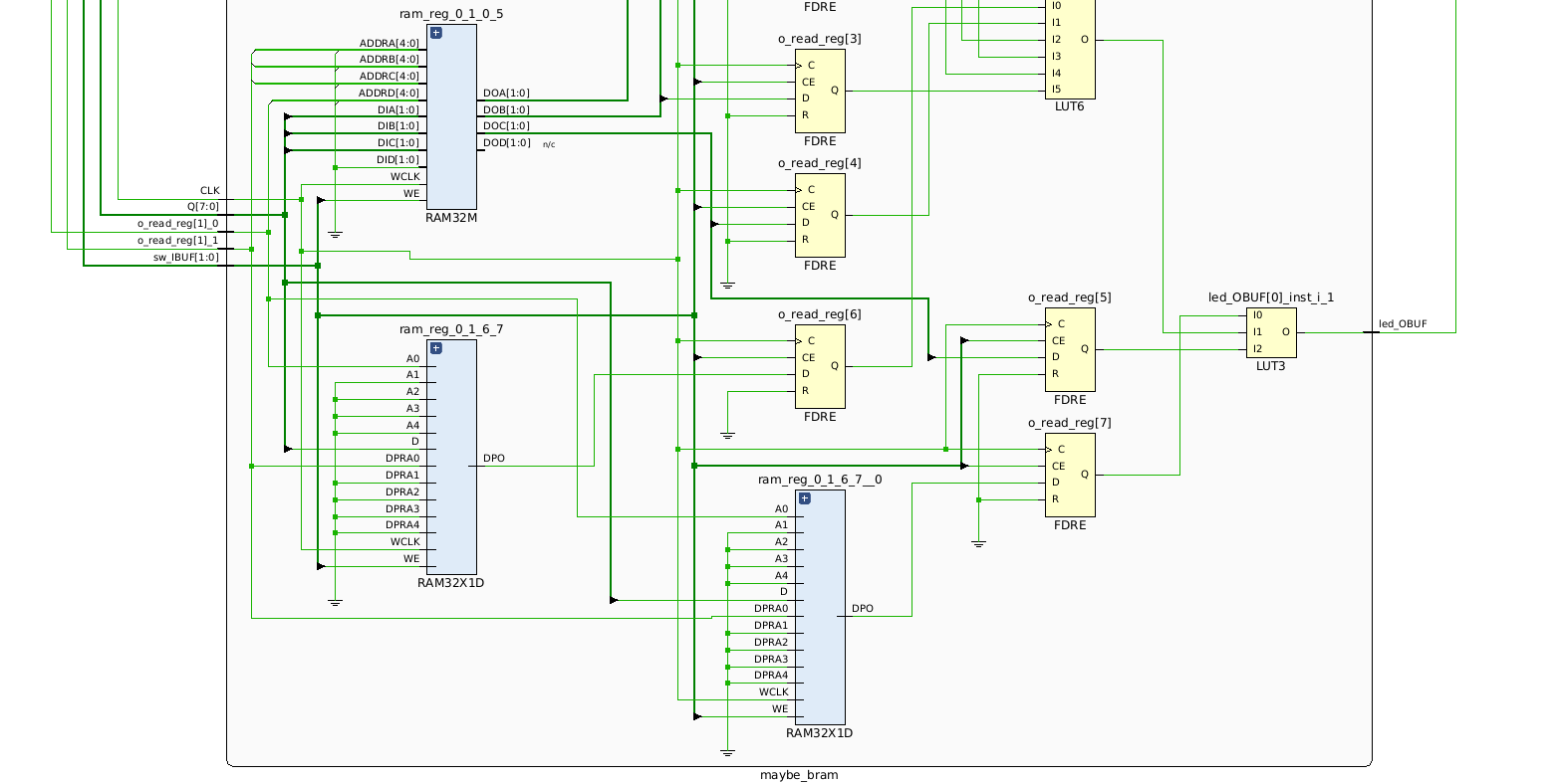
Schematic view of the
maybe_bramVerilog module.
The RAM32M element is described as follows in the Xilinx docs:
This design element is a 32-bit deep by 8-bit wide, multi-port, random access memory with synchronous write and asynchronous independent, 2-bit, wide-read capability. This RAM is implemented using the LUT resources of the device known as SelectRAM™+, and does not consume any of the Block RAM resources of the device.
Expanding the element reveals the underlying LUT primitives.
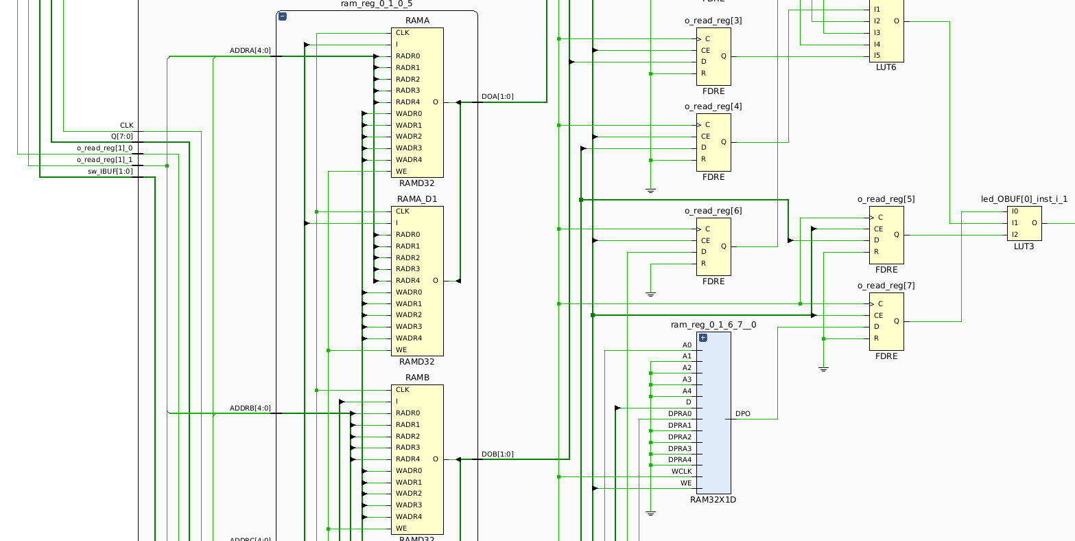
Expanded schematic view of a
RAM32Melement.
However, rather than being labeled as LUT elements, they are named RAMD32. On
Xilinx 7 Series FPGAs, LUTs reside in either a SLICEL or SLICEM, with the
L suffix denoting “logic” and the M denoting “memory”. Each slice has 4
6-input LUT elements (i.e. LUT6). In SLICEM slices, the LUTs can be
configured as distributed memory. RAM32M elements use all 4 LUTs on a SLICEM
slice.
By our earlier calculation, a
LUT6element has2^6 = 64initial values.
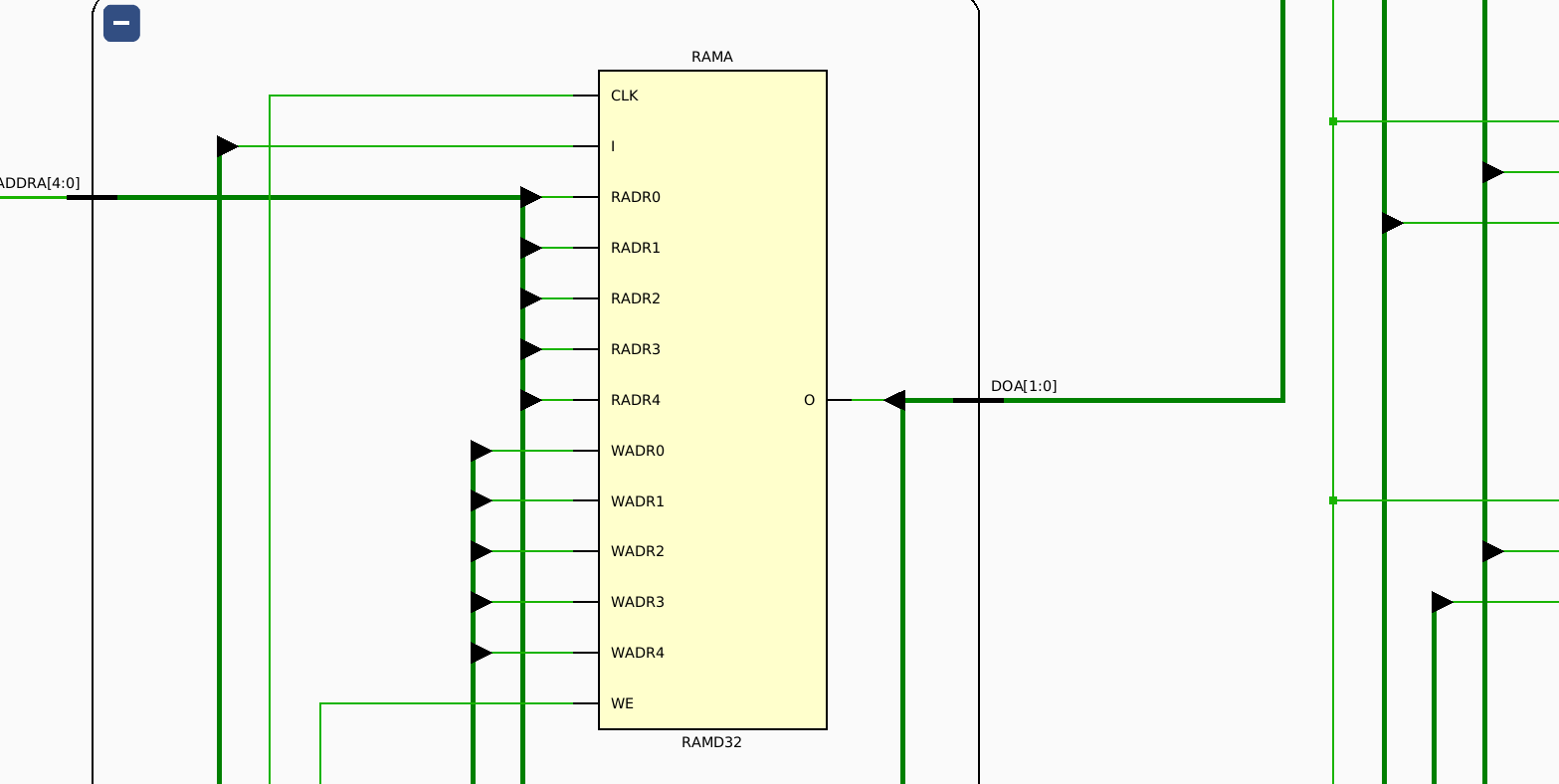
As can be seen in the schematic, the LUTs support 5 read address ports (RADR)
and 5 write address (WADR). Though SLICEM slices contain 6-input LUTs, a
LUT6 is just two LUT5 elements wired
together,
so a single RAMD32 refers to a LUT5 configured as distributed RAM. We see 8
LUT5 elements making up a RAM32M distributed memory (4 LUT6 elements, each
comprised of 2 LUT5 elements).
Schematic view of a
LUT5acting as a distributed memory component (RAMD32).
If we look at the same elements on the device, we can see the LUT5 within the
LUT6.
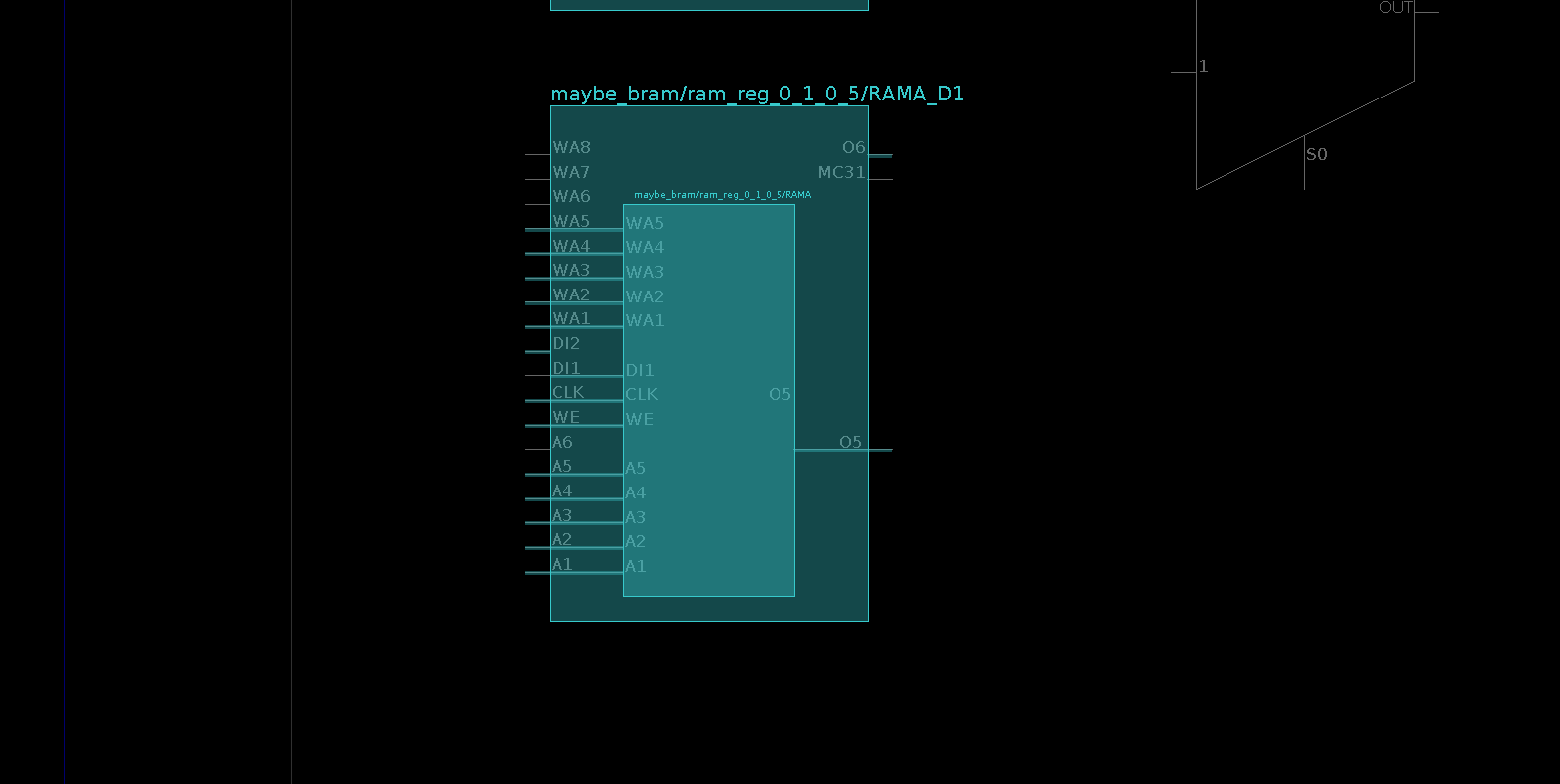
Device view of the same
RAMD32/LUT5element shown in the schematic above.
Note: I am assuming the reason only one
LUT5is shown within theLUT6is because the device footprint is static in Vivado (i.e. implemented designs are just shown by highlighting the elements in use), and “wrapping” theLUT5in theLUT6somewhat illustrates that aLUT5could be used individually or as part of aLUT6. Feel free to reach out if you have an alternative explanation!
Zooming out further, we can see the 4 LUT6 elements in both SLICEM and
SLICEL slices.
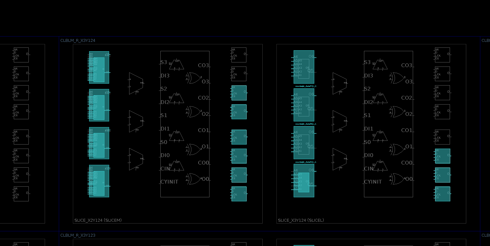
Device view of one
SLICEM(left) and oneSLICEL(right), each with 4LUT6elements, but only theSLICEMLUTs showing write address ports.
However, the SLICEM LUTs, as previously mentioned, also support writing, which
is why we see the additional WADR address lines, as well as a write enable
(WE) and write clock (WCLK) signal. The comparison between BRAM and
distributed RAM in our earlier post identified that, with BRAM, read and writes
are both synchronous, whereas with distributed RAM writes are synchronous, but
reads are asynchronous. In order to implement the synchronous writes, a clock
signal (WCLK) is required.
Note: synchronous reads can be implemented with distributed RAM, as evidenced by our example where we forced distributed RAM usage. Doing so requires connecting the output to a flip-flop in the same slice.
Though it may be obvious at this point, the reason why these LUTs can be used
as distributed RAM is because we already need to be able to write values to
LUT SRAM to configure the FPGA. When they are used as distributed RAM, we use
that same functionality to write values after configuration. The
aforementioned “initial values” (i.e. INIT[X]) are not only available for
reading, but also for writing.
Closing Thoughts Link to heading
Small realizations about the physical characteristics of a device can help us
develop a better intuition about why designs are being implemented in a certain
manner, as well as the tradeoffs of using different types of components. These
are the tedious details that I hope to continue to capture via
livestreams and posts in this
series (RSS
feed), while developing
expertise in chip
design and
building the moss project.
As always, if you have feedback, questions, or just want to chat, feel free to
reach out to @hasheddan on any of the platforms listed on the home
page.